
Anil Pandey's Blog: Interview With Author Anil Pandey
June 20, 2023
Quantum Chip Designs
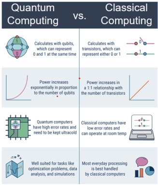 With industries powered by 6G, artificial intelligence (AI) and the internet of things (IoT) on the rise, the enabling possibilities that quantum technology could bring about will make it highly desired by companies globally. Quantum and classical computers both try to solve problems, but the way they manipulate data to get answers is fundamentally different.
Quantum technology is still in the early stages of commercializing, but the quantum race has begun, and several companies have jumped on board. With the investment of tens of billions of dollars from academia, venture capitalists and governments, it is highly likely that quantum computing will grow very fast in coming years.
Need for Quantum TechnologyMany real-life problems in several areas, such as planning, manufacturing, complex diseases, DNA sequencing, … etc., are intractable to solve with current technology. Another challenge with current computational technology is that transistors is reaching a limitation — fundamental limit of reducing the transistor size is soon coming, end of Moore’s law!
Quantum ConceptsA classical computer uses bits that are represented as either a 0 or 1, to perform its operations. Quantum computers on the other hand uses “qubits,” meaning that the data is stored in a state of superposition that can represent 0, 1 or 0 and 1 in tandem. This allows qubits to process information in parallel.
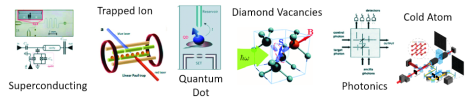
Superconductors – At those ultra-low temperatures in certain, electrons move through them without resistance. This makes them “superconductors.”Superposition – Superposition is a quantum system’s ability to be in multiple states at the same time before researchers take any measurements.Entanglement – Entanglement is a quantum mechanical effect that correlates the behavior of two separate things. When two qubits are entangled, changes to one qubit directly impact the other.Interference – In quantum, interference is used to affect probability amplitudes. There are two kinds of quantum interference: constructive interference and destructive interference.Control – quantum computers use Josephson Junctions as superconducting qubits. By firing microwave photons at these qubits, we can control their behavior and get them to hold, change, and read out individual units of quantum information.Quantum Computing by TechnologyThere are at least six major quantum technology approaches being explored worldwide: superconducting qubits, silicon spin qubits, ion traps, , diamond vacancies and topological qubits.
Qubits – Superposition of supercurrents flowing around a Superconductor.Trapped Ions– Superposition of trapped ions states, ions are trapped with electric fields.Quantum Dots– Superposition of electron spin states, electrons are trapped in a solid substrate.Diamond Vacancies– Superposition of electron spin states, electrons are created with NVs in a solid substrate.Photonics-Quantum states of photons travelling around circuits in silicon chips.Cold Atoms-Superposition of cold natural atoms quantum states


April 28, 2020
Array Antenna: Taylor Synthesis for Low Sidelobe Level (SLL) using Matlab Code
Antenna array is one of the most useable technologies in modern and latest communication systems like 5G. The 5G communications adopt the millimeter wave (mm-wave) and beamforming technologies based on antenna arrays, to improve the spectral efficiency and communication rate of the system. Antenna arrays are used to obtain narrow beamwidth, high directivity, beamforming and low side-lobes pattern characteristics. In many applications, low sidelobe level (SLL) is an essential feature of beamforming array antenna system. A directional main lobe with the low SLL of the beam pattern will effectively enhance the communication quality and reduce the interferences. There is a trade-off between the directivity of the array and SLL.
Over the years, some key optimization techniques have been developed to suppress high SLL of antenna beam pattern. Amplitude weighting of array elements is a popular approach for SLL reduction. The technique of amplitude-only control is a simple method as it changes only the current amplitude excited at each element. By amplitude tapering of the array elements, the SLL of the array can be suppressed. Taylor amplitude excitation yields a pattern that is an optimum compromise between directivity and SLL.
Matlab CodeLanguage: Matlab (2018B)Download: Matlab code is given belowOutput Plot[image error]Output of Taylor Synthesis
———————Matlab Code————–function [fm,im] = taylorsyn(N,SLL,nb,dx) % Array antenna Tayler synthesis for low side lobe level% Program written by: Anil Kumar Pandey %#######################################################################% This function written in matlab, calculates Linear antenna array pattern coefficient base on Taylor Line source synthesis% Example: run this in command line taylorsyn(32,-30,16,.8)%#######################################################################
clear all;format short; % N=input(‘Enter number of elements=’);% SLL=input(‘Enter the value of SLL=’);% nb=input(‘Enter the value of nbar=’); N=18;SLL=-40;nb=10;dx=0.8;lambda=1;L=(N-1)*dx*lambda;R=10.^(-SLL/20);A=(1/pi)*acosh(R);nb_check=(2*A^2) 1/2;fm=[]; if nb >= nb_checkfor m=1:1:nb-1c1= ((factorial(nb-1))^2)/((factorial(nb-1 m))*(factorial(nb-1-m)));c2_s=[];
st=0;for n=1:1:(nb-1)nw= nb/(sqrt(A^2 (nb-1/2)^2));zn= nw*sqrt(A^2 (n-1/2)^2);c2= (1-(m^2/zn^2));c2_s=[c2_s c2];endst=prod(c2_s);fmv=st*c1;fm=[fm fmv];endelsesprintf(‘Error: Wrong nb, please select proper value of nb’)end
fm
%—————-Arranging coefficient for all elements——————-
fm3=[];for k2=1:1:nb-1fm2=fm(nb-k2);fm3=[fm3 fm2];endfm3=[fm3 1];fm4=[];for k2=1:1:nb-1fm2=fm(k2);fm3=[fm3 fm2];end%————–Current Distribution Cal ———————-
im=[];s2=[];for s=-L/2:dx:L/2s2=[s2 s];ssum=0;a1=lambda/L;for k=1:1:nb-1 a2=fm(k)*cos(2*pi*(lambda/L)*k*s);ssum=ssum a2;enda3=a1*(1 2*ssum);im=[im a3];endimim_v=im./max(im);%—————Pattern calculation —————
dd=max(size(fm3));bb=[];ww=[];pth=[];for w=-1:.01:1 ww=[ww w];ss=0;for n=((-nb 1):1:(nb-1))b1=sin((w-(lambda*n/L))*L*pi/lambda)/((w-(lambda*n/L))*L*pi/lambda);n2=n nb;b2=fm3(n2)*b1;ss=ss b2;endss=ss;pth=[pth ss];end%—————Half Power beamwidth —————————
HPwi=((2*lambda)/(L*pi))*sqrt((acosh(R))^2-(acosh(R/(sqrt(2))))^2);HPi=2*asin((lambda/(L*pi))*sqrt((acosh(R))^2-(acosh(R/(sqrt(2))))^2))*180/pi;HPw=nw*HPwi;HP= 2*asin((lambda*nw/(L*pi))*sqrt((acosh(R))^2-(acosh(R/(sqrt(2))))^2))*180/pi;%———————–All Data Plots————————————
mFigure = figure(‘Name’, ‘Linear Array Synthesis using Taylor Line Source ( Anil Pandey)’,…
‘color’,[1,1,1],‘units’,‘centimeters’,‘resize’,‘off’,‘position’,[1 1 25 18]);
subplot(2,2,1);%Current Distribution Plot
plot(s2,im,‘–rs’,‘LineWidth’,2,…
‘MarkerEdgeColor’,‘k’,…
‘MarkerFaceColor’,‘g’,…
‘MarkerSize’,10)
xlabel(‘L:(Line source length)’)
ylabel(‘Im(Current Distribution)’)
title(‘Current Distribution Plot’)
grid on
subplot(2,2,2);%Normalized Current Distribution Plot
plot(s2,im_v,‘–rs’,‘LineWidth’,2,…
‘MarkerEdgeColor’,‘b’,…
‘MarkerFaceColor’,‘r’,…
‘MarkerSize’,5)
xlabel(‘L:(Line source length)’)
ylabel(‘Normalized Im(Current Distribution)’)
title(‘Normalized Current Distribution Plot’)
grid on
subplot(2,2,3); %Radiation Pattern Plot
pth2=abs(pth/max(pth));
pth3=20*log10(pth2);
plot(ww,pth3,‘LineWidth’,2)
xlabel(‘w=cos(theta)’)
ylabel(‘f(w)[dB]’)
title(‘Radiation Pattern Plot’)
grid on
%————————-Text data in figure——
htitle = text(‘units’,‘centimeters’,‘FontWeight’,‘bold’,‘position’,[6 15.7],‘fontsize’,11, ‘string’,‘Taylor Line Source Synthesis’);
htitle = text(‘units’,‘centimeters’,‘FontWeight’,‘bold’,‘position’,[12.5 6.2],‘fontsize’,11, ‘string’,‘———Synthesized Data———‘);
h2 = text(‘units’,‘centimeters’,‘Position’,[10 5.4],‘Fontsize’,11,‘String’,‘Number of Elements =’);
h3 = text(‘units’,‘centimeters’,‘Position’,[14.5 5.4],‘Fontsize’,11,‘String’,N);
h4 = text(‘units’,‘centimeters’,‘Position’,[10 4.8],‘Fontsize’,11,‘String’,‘Value of SLL =’);
h5 = text(‘units’,‘centimeters’,‘Position’,[14.5 4.8],‘Fontsize’,11,‘String’,SLL);
h6 = text(‘units’,‘centimeters’,‘Position’,[10 4.2],‘Fontsize’,11,‘String’,‘Value of nBar =’);
h7 = text(‘units’,‘centimeters’,‘Position’,[14.5 4.2],‘Fontsize’,11,‘String’,nb);
h8 = text(‘units’,‘centimeters’,‘Position’,[10 3.0],‘Fontsize’,11,‘String’,‘Half Power beamwidth (HPwi) =’);
h9 = text(‘units’,‘centimeters’,‘Position’,[16 3.0],‘Fontsize’,11,‘String’,HPwi);
h10 = text(‘units’,‘centimeters’,‘Position’,[10 2.4],‘Fontsize’,11,‘String’,‘Half Power beamwidth (HPPi) =’);
h11 = text(‘units’,‘centimeters’,‘Position’,[16 2.4],‘Fontsize’,11,‘String’,HPi);
h12 = text(‘units’,‘centimeters’,‘Position’,[10 1.8],‘Fontsize’,11,‘String’,‘Half Power beamwidth (HPw) =’);
h13 = text(‘units’,‘centimeters’,‘Position’,[16 1.8],‘Fontsize’,11,‘String’,HPw);
h14 = text(‘units’,‘centimeters’,‘Position’,[10 1.2],‘Fontsize’,11,‘String’,‘Half Power beamwidth (HP) =’);
h15 = text(‘units’,‘centimeters’,‘Position’,[16 1.2],‘Fontsize’,11,‘String’,HP);
h16 = text(‘units’,‘centimeters’,‘Position’,[17 0],‘Fontsize’,11,‘String’,‘(c) Anil Kumar Pandey’);
February 18, 2020
Waveguide to Microstrip Line Transitions for mmWave Applications
Author: Anil Pandey
An increasing number of RF and Microwave applications at the sub-millimeter and millimeter frequency ranges in different fields such as communications, imaging, automotive radar and tracking radar has increased the demand for the components and systems in this range. To handle the high-power requirement in these frequency ranges, waveguide-based components are used as a power feed network. In the mmWave, the waveguide is normally adopted as the main transmission line instead of a coaxial cable due to easier manufacturability and lower loss. Components based on planar technology like monolithic microwave integrated circuits (MMICs) are relevant. Therefore, a low insertion loss and broadband transition between the microstrip line and waveguide is very crucial for these applications. In addition, at millimeter and terahertz frequencies, most measuring equipment is waveguide-based due to the lack of connectors that’s why the transition is needed. There are several types for microstrip-to-waveguide transitions based on the application like the design based on the ridged waveguide, antipodal finline, coupling probe, dipole antenna, substrate integrated waveguides (SIW), iris coupling, etc.
Design-1: E-Plane Probe Transition with Back Short
Among these, the E-plane probe coupling method is very frequently used. In this transition, a microstrip line is inserted through an aperture in the E-plane of a rectangular waveguide that couples TE10 mode of the waveguide to the quasi-TEM mode of the microstrip line. In the E-plane probe transition network, the input port is perpendicular to the output port, sometimes this makes the realization of devices or antennas very difficult in limited space as addition bends are required. This transition consists of a printed probe on one side of the dielectric substrate inserted into rectangular waveguide with back short. This type of transition is very sensitive to the position of the dielectric substrate and microstrip line with respect to the waveguide. However, there are some drawbacks to this type of transition. The channel width and height, that holds the microstrip substrate and the E-plane probe, should be very small so that all the waveguide modes are under cut-off and only the microstrip quasi-TEM mode can propagate within the band of operation.
Below is the design of a waveguide-to-microstrip transition based on the E-plane probe, designed in mmWave (65-85 GHz) for automotive radar applications. A coupling probe at one end of the microstrip line is introduced into the perpendicular waveguide through an aperture in the waveguide broad wall. The copper probe is designed as a rectangular sheet. One end of waveguide is short-circuited by the metallic plate. Liquid Crystalline Polymer (LCP) is used as the substrate material for reducing the transition loss. The thickness of the substrate is set as 0.79mm. The microstrip line characteristic impedance is 50Ω. The distance between the probe center and the waveguide back-short is a quarter of the WR12 waveguide wavelength at 75 GHz. The aperture size is optimized to guide the wave coupled to the microstrip line effectively and to minimize its effect on the field distribution in the waveguide.
[image error]Lateral radiation introduce leakage that is suppressed by using stitching vias to connect both side of ground planes on the substrate with the upper and lower waveguides. Also, in order to reduce the leakage from the waveguide opening window, the width of the opening should be smaller than the width of the cut-off condition. A radial stub has been used at the end of the probe to match the impedance of the network for broadband performance.[image error]
S-parameters of the return loss S11 and the transmission loss S21 are calculated by a full-wave Finite Element Method (FEM) based electromagnetic simulator. The simulation result of the waveguide-to-microstrip transition is shown in Fig. 3. The return loss is less than -20 dB within 62 GHz – 78 GHz. The maximum return loss is -22.8 dB at 73 GHz. The insertion loss is greater than -0.21 dB within 62-78 GHz. The minimum insertion loss is -0.1 dB at 73 GHz. The bandwidth of the transition is about 22% for less than -20 dB return loss.
[image error]The electric current on the metallic probe couples to the magnetic field of TE10 dominant mode of the rectangular waveguide as shown in below picture. Via holes reduces the leakage of parallel plate mode transmitting into the substrate. Impedance matching is achieved by controlling the length of the probe and the distance of the back short waveguide.
[image error]
Design-2: Half-Height Waveguide to Microstrip Line Transition
To reduce the transition dimension and simply the design, a half-height rectangular waveguide to microstrip line transition network is used. The gradual transition from the microstrip line to the waveguide is used to transfer impedance smoothly. The reflection coefficient at the feed point depends on the probe length, a distance of the waveguide short and probe width. To make sure the efficient electric coupling, the probe is always located at the maximum electric field in the structure. The below figure shows the electromagnetic simulation model of half-height waveguide WR12 to 50Ω microstrip line. The planar circuit is supported on a quartz substrate or 10 mils. The copper probe patch is perpendicularly inserted into the center of the broad wall. The plane is perpendicular to the transverse section and parallel to the E-plane of the half-height waveguide. It can be noted that in design-1 discussed above, Microstrip probe is perpendicular to E-plane.
[image error]
The simulation result of the back-to-back design is shown in the below figure. Based on FEM solver results, it is found that transition structure has S11 better than -20 dB from 70 GHz to 80GHz. S12 is less than 0.12 dB over the operating frequency band.
[image error]
Design-3 Oversized Waveguide to microstrip line transition for Radial Power combiner/ divider
Power amplifiers (PA) are found in several millimeter-wave systems. Radar and satellite communications are two systems where high-power is very important. MmWave communication systems require high transmitter power because atmospheric attenuation at mmWave (60GHz) frequency is quite high. The power needs at this frequency are up to several watts and a single Solid-State Power Amplifier (SSPA) cannot meet this requirement. Radial high-power combing technology overcomes this design challenge. Radial divider/combiner distributes the signal of one common input port to the N-output waveguides cavity. This power is coupled with a cavity microstrip line resonator and supplied to SSPA. The output of SSPAs is again supplied to N-Waveguides that are combined to a single output port as shown in the figure. The radial divider/combiner does not use corporate or cascaded structures and, thus, routing losses are minimized, and overall insertion losses of the whole structure are very low.
[image error]Axially symmetric oversized coaxial waveguide power combiner utilizes a planar microstrip probe to transform TE10 mode to quasi TEM mode. This transition network has broadband with high-efficiency performance, which has been used widely in many mmWave systems. To provide a smooth impedance match from the input port to the oversized coaxial waveguide, a nonuniform coaxial taper transition circuit is used. The inner conductor is inserted into the center of the gradual taper in order to provide a perfect electrical connection. The outer and inner conductors of the coaxial taper transition have been tapered at two different planes rather than on the same plane, which can provide a good impedance match.
[image error]The simulated return loss and insertion loss plot of the planar probe combiner are shown in the below figure. Return loss (S11) is better than -10dB over the band (62 GHz to 87 GHz) giving wideband (35% bandwidth) performance. The isolation between the peripheral ports is better than 12 dB. This type of radial power combiner/divider establishes the advantages of easy design and fabrication, perfect compatibility with the mmWave integrated circuitry, low insertion loss and high power-combining efficiency.
Design-4 In-Line Stepped Transformation H-plane Waveguide to Microstrip line Transition
The TE10 rectangular waveguide mode can be coupled to quasi-TEM of microstrip mode by using inline configuration. In this design, the field propagation direction in the microstrip line is the same as the waveguide. A wideband impedance transformer using stepped ridge waveguide provides excellent transition performance. Ridge waveguide has a smaller equivalent impedance which is easier to match with the coaxial and microstrip line. Waveguide to Microstrip line transition is designed using a multi-section stepped transformer as shown in Figure. In this design, the inner coaxial conductor extends across the interior of the waveguide to terminate on a metallic probe to assist in impedance tapering. An in-line waveguide-to-microstrip transition design was proposed by Yao [3] in 1994.
The probe is built using a microstrip line matched to the waveguide through a ridged configuration, on which the microstrip line is attached as shown in the below Figure. A Chebyshev 4-section impedance transformer provides the matching from the stepped transition to the full waveguide. The probe lies on a plane parallel to the wide side of the waveguide and it is inserted from the back-short of the waveguide such that the E-planes of the two devices are parallel. The microstrip line is centered along the wide side.
[image error]
The design is simulated using a FEM solver. A return loss greater than -15dB over the entire operating band (71 GHz to 79 GHz) is obtained for back-to-back configuration as shown in the below picture. The insertion loss is lower than 0.2, so a good power transmission is provided.
[image error]
Design-5 Inline Waveguide to Microstrip line transition using a Slope-Probe
Fabrication of stepped ridge probe, discussed in design-4, is difficult, and dimensions are sensitive to result. Instead of the stepped transformer, a smooth copper transition as shown below in the picture can be used to match waveguide impedance to microstrip line impedance. In this way, the fundamental TE10 mode of the rectangular waveguide is converted progressively to the quasi-TEM microstrip mode in a broadband inline configuration. The microstrip line is printed on a dielectric substrate and the end of the substrate along with the cavity enclosure is narrowed to concentrate the fields near the metallic strip. The short portion of the microstrip line is inserted into the waveguide and placed seamlessly underneath the probe.
[image error] [image error]
Design-6: Inline Waveguide to Microstrip Line Transition through a Coaxial Line
Wheeler [2] first investigated In-line waveguide transitions in the 1950s, when he studied the transition from waveguide to a 50 ohms coaxial line. Waveguide to Microstrip line (through SMA connector line output port) transition is designed using a multi-section stepped transformer as shown in Figure. In this design, the inner coaxial conductor extends across the interior of the waveguide to terminate on a metallic probe to assist in impedance tapering.
[image error]
Design is based on two key factors; the first factor is mode conversion from the dominant mode of the input transmission medium to that of output transmission medium and impedance matching is the second facto. In rectangular waveguide to coaxial line transition, TE10 mode in the waveguide is converted to the TEM mode of the coaxial line. The characteristic impedance of rectangular waveguide is a function of frequency. Therefore, to match the rectangular waveguide impedance to the 50 Ω coaxial line impedance over the desired frequency range, a multi-step matching transformer is needed. Simulated return and transmission loss are shown below in the figure.
[image error]
In some applications, microstrip antennas are placed on the top surface of design and are fed with an in-line waveguide as shown below in the figure. One advantage of such design is that it can be easily integrated with the Microstrip feed-line of antenna or can be directly connected to patch antenna.
[image error]
Design-7 E-Plane Waveguide to Microstrip line transition through Coaxial line
In the E-plane transition referred to as orthogonal transition, the center conductor of the probe (coaxial line) is inserted into the waveguide. This excites the TE01 mode in the waveguide. The probe is placed in such a way that the reflected EM fields get combined in phase with the incident EM fields. The distance between the back wall and probe center is optimized to achieve good impedance matching. Typically, it is kept at λg/4. E-plane probe is the most popular type of transition but it gives narrow band performance unless additional matching elements are included which increases the physical size. The coaxial-line and probe are perpendicular to microstrip and waveguide. The probe is inserted to the waveguide at the center of the waveguide wide side. S11 result is shown in the figure that is better than -10 dB in all the band of interest.
[image error]
References
[1] A. Pandey, Practical Microstrip and Printed Antenna Design, Artech House, Norwood, MA, 2019.
[2] Wheeler, G. Broadband waveguide-to-coax transitions. In Proceedings of the 1958 IRE International Convention Record, New York, NY, USA, 21–25 March 1966; Volume 5, pp. 182–185.
[3] Yao, H.-W.; Abdelmonem, A.; Liang, J.-F.; Zaki, K.A. Analysis and design of Microstrip-to-Waveguide Transitions. IEEE Trans. Microw. Theory Tech. 1994, 42, 2371–2380.
[4] A. K. Pandey, “Design of a cosecant square-shaped beam pattern SAR antenna array fed with square coaxial feeder network,” 2013 European Microwave Conference, Nuremberg, 2013, pp. 1699-1702.
February 9, 2020
Energy Harvesting and Wireless Power Transfer Antenna for IoT Applications
Several processes that include energy conversion, there is energy waste in the form of heat, like power amplifiers, automobile engines, light bulb and electrical motor get hot and energy is wasted. Energy harvesting devices capture some of these wasted energy from one or more renewable energy sources (like light, vibration, RF, motion, heat etc.), convert it to back into electrical energy. Energy harvesting (EH) is also known as micro energy harvesting or energy scavenging, is defined as the process of capturing energy from the surroundings of a system and converting it into usable electrical energy. The electrical energy is conditioned for either direct use or accumulated and stored for later use. This provides an alternative source of power for applications in locations where there is no grid power and it is inefficient to install wind turbines or solar panels. Based of energy source, there are several energy harvesting types:
Light: From sunlight or indoor lighting
Kinetic energy: From mechanical stress/strain or vibration
Thermal: Energy from thermal sources like heaters, engines, friction, furnaces, etc.
RF: From radio-frequency signals[image error]
Solar: Solar energy is converted into electrical energy by using photovoltaic (PV). These polycrystalline silicon or thin-film cells convert photons to electrons with a typical efficiency of about 10-20% for polycrystalline and 5-12% for thin film cells. Solar power can provide an unlimited level of energy to IoT and embedded platforms if there’s sunlight but since light sources tend to be irregular, solar cells are used to charge batteries to provide a stable energy source.
Thermoelectric: Thermoelectric harvesters are based on the Seebeck effect, where a voltage is generated when there is a temperature difference at the junction of two dissimilar metals. Generally, thermoelectric generators (TEG) contains silicon nanowires of 10-100 nm length and these wires are suspended over a cavity. An array of these TEGs are connected in series to a common heat source such as water heater or engine. Total output power depends on the temperature differential and the size of the TEG array.[image error]
Piezoelectric: When piezoelectric transducers are stressed, they generate electrical energy. These transducers are used as vibration sensors to detect vibration of aircraft [image error]wings, sound, motor bearing noise or any other kinetic energy. Because of kinetic energy, the movement of cantilever generates an AC output voltage. This voltage is rectified, regulated, and stored in a thin-film battery or super capacitor. Piezoelectric sensors are put inside the car tire where they do energy harvesting to monitor tyre pressure and transmit the information.
Radio Frequency – RF: Radio frequency (RF) energy harvester captures RF signals and generate useful electrical power. These are very attractive for low-power electronic devices and wireless sensor networks (WSNs). A typical RF energy harvesting system consists of a receiving antenna, peak detector, matching circuit, and voltage elevator. Antenna captures the electromagnetic waves and converts into RF signal. By using a matching circuit and peak detector, this signal is converted to a voltage value. Finally, this voltage output is adjusted using the voltage elevator.
Energy Harvesting for IoT Devices:
Low power is one of most important electronic design criteria special in IoT devices. These devices often consume in active operating mode and nano-watts in standby or non-operating mode. It is required to extend the battery life by harvesting environmental energy sources – most often available as heat, light, heat, motion, vibration, or ambient RF. For low power IoT devices if battery replacement is difficult or expensive then it is possible to rely completely on harvesting ambient energy sources for power without any battery. The energy harvesting together with ultra-low-power microcontroller unit (MCU) for open the door for many applications that previously were not possible. Even though the power is usually harvested in small amounts, it is adequate for various low-power applications. The power-management integrated circuits (PMC ICs) manages ultra-low-power applications and ensure efficient use of the harvested energy.
Wireless power transfer (WPT) in IoT applications
Wireless energy harvesting (WEH) or green energy harvesting is used to convert RF energy into electrical energy. In WPT system, electric energy is transmitted without conducting wires. A transmitter driven by electric power source, generates electromagnetic field. This electromagnetic field (power) is transmitted in the free space and a receiving device extracts this power from the electromagnetic field and convert back to electrical power. Nikola Tesla first worked on WPT technology in 1890 and he was able to transmit electric energy from one coil to another coil. WPT is an alternate solution to energy harvesting when the environmental energy not enough. For IoT devices, WPT technologies and energy harvesting are very good renewable and clean power source. Implantable electronic devices and RFID tags are also used as RF power harvesting method. Selection of frequency-band is a vital consideration in RF power harvesting systems. For energy harvesting systems any frequency band can be used but most readily available bands are Wi-Fi hotspots, cellular (850/900 MHz band), PCS (1800/1900 MHz band), WiMAX (3.5/2.3 GHz) and 2.4 GHz network transmitters.
Rectenna:
In case of IoT applications, an antenna system (called rectifying antenna or rectenna) is used to charge remotely placed batteries wirelessly. The radio-frequency (RF) energy from neighboring sources, such as nearby wireless local area networks (WLANs), cellphones, Wi-Fi, DTV, and FM/AM radio signals, is collected by a receiving antenna and rectified into DC voltage. Rectenna is has two main elements: (1) the antenna that receives the electromagnetic waves and convert in a RF/microwave signal and (2) the rectifier that changes RF signal into direct current (DC). DC power depends on several factor such as the available RF power, the choice of antenna, frequency band, and the energy harvesting technique.
[image error]
For rectenna design, microstrip patch antennas are widely used because these are planar, low profile and lightweight structure. Design of rectenna with wide bandwidth and high gain is crucial to maximize the received power. Efficiency of the overall system greatly depends upon the matching between the rectifier and antenna. System efficiency is further limited by variable input impedance with frequency of the rectifier.
[image error]
Nantenna:
A nantenna (nanoantenna) is a nanoscopic rectifying antenna. At high-frequency, semiconductor-based solar cells and very small (nanoscale) antennas for power harvesting applications are gaining research interest. These nanoantennas transform thermal energy into electrical energy. Nanoantennas are designed at the infrared (IR) wavelengths. At these frequencies (terahertz radiation), traditional photo-voltaic cells are not very efficient. Nantenna is an electromagnetic collector that absorb specific wavelengths those are proportional to the size of the nanoantenna. The MBE (molecular[image error] beam epitaxy) technique is used to AlGaAs/GaAs-stamps which are used to fabricate nano antennas. MBE-fabricated MOM (metal-oxide-metal) diodes having spatial dimensions in the nanometer range, is use for in nano antennas. For rectifying THz electromagnetic radiation, MOM tunneling diodes are printed having an ultrathin dielectric.
January 16, 2020
Antenna Design with Machine Learning
Over the past few year, machine learning has attracted the attention of antenna engineers. Generally, the process of antenna design requires to find out the EM characteristics of antenna by observing the current distributions through simulations. These EM properties are then used for the parameters optimization. Machine learning (ML) can be combined with simulations to design an antenna. The inclusion of artificial intelligence (AI) can give promising results in the field of antenna designing. In recent years, antenna synthesis or design optimization through evolutionary algorithms (EAs) has been applied widely. At present, differential evolution (DE) and particle swarm optimization (PSO) are top two popular algorithms in the antenna synthesis area.
In smart antenna array, the objective of the gracefully degradation of the beamforming and beamsteering performance, can be achieved by reconfiguring the array when an element is found to be defective. This reconfiguration can be obtained by optimization using Machine learning and Support Vector Machines (SVM). SVMs are a set of supervised learning algorithms used for classification and regression problems. SVMs are a good candidate for the solution of antenna array processing problems such as beamforming and the angle of arrival estimation, because these algorithms provide superior performance in generalization ability and computational complexity. The basic idea is to change the excitation coefficient for each array element (magnitude and phase) to optimize for changes due to the environment surrounding an array antenna. Using Support Vector Machines, the antenna array is trained to change its elements phase or excitation distribution to maintain a certain radiation pattern or to enhance its beam steering and nulling properties and solve the DOA problem as well.
Optimization technique based SVMs algorithm is also used to match the measured far field radiation intensity to the corresponding antenna array structure. The SVM classifier is firstly trained by a set of input feature vectors extracted from measured radiation data of different array structures in various scenarios. Then, it is tested and the SVM parameters are adjusted during the learning process to help approach the optimal classification result. Then the trained SVM classifier is used to locate malfunctioning antenna elements of the array in real-time.
Machine learning based methods are used for calculating the radar cross section (RCS) of the antenna-radome system. In this method, the back-propagation algorithm can be used to train the machine learning model. The machine leaning based RCS calculation becomes a promising area, especially for the industrial sector with large amount of measurement data. Compared to traditional methods, machine learning methods have the potential to handle complex.
Machine learning techniques are also efficient in shaped-beam array designs. Here, SVM is applied for the characterization of the reflection coefficient matrix, which provides an efficient way for deriving the scattering parameters associated with the unit cell dimensions. ML is one of the most promising and salient research areas in artificial intelligence, as it has become a powerful tool in a wide range of antenna designs and related applications.
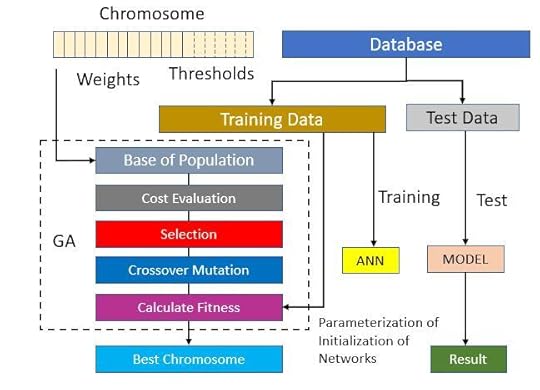
Genetic algorithm (GA)Genetic algorithm (GA) is one of the global optimization algorithms that is used widely by antenna designers for the optimization of the antenna shape and size to achieve better overall performance of the antenna. GA has been used to enhance the performance of microstrip patch antennas by optimizing the bandwidth, multi-frequency, directivity, gain, size etc. The concept of the GA, first formalized by Holland and extended to functional optimization by De Jong, involves the use of optimization search strategies patterned after the Darwinian notion of natural selection and evolution.
During a GA optimization, the parameters of each individual of the population are encoded as a string of bits (chromosomes). The first group of individuals (generation) is created randomly. The fitness of each individual is determined by the cost function. Mating these individuals forms a new generation. The more fit individuals are selected and given greater chance of reproducing. Crossover and mutation are used to allow global exploration of the cost function. The best individual may be passed unchanged to the next generation. This iterative process creates successive generations until a stop criterion is reached. A block diagram of a genetic algorithm optimizer is shown here.
December 25, 2019
Top 10 Technology Trends for 2020
Innovation is advancing quicker than ever. As technology advances, it enables even faster change and progress, causing an acceleration of the rate of change, until eventually, it will become exponential. Engineers and researchers that don’t stay aware of some of the significant-tech patterns take the risk of being abandoned. Understanding the key patterns will enable individuals and researchers to plan and embrace opportunities.
There are many such technologies that have already made their prominent mark in 2019 and are only a few more applications away from becoming mainstream like 5G. Artificial Intelligence is one of the fast-growing technology for the future. The technology, with its potential to mimic the human brain, has offered numerous opportunities to different areas. Distributed ledger technology such as artificial intelligence (AI), blockchain, virtual and augmented reality, and Quantum computing, abbreviated to DARQ form one such future technology trend of 2020 that business must integrate on priority.
There are some technology trends that fizz out over time and then there are the latest technology trends that stay on the sidelines and then gain traction after an industry suddenly integrates it in their process. Technology trends in 2020 will come with both profound innovation and complex connectivity. Democratization would empower engineers to create data models without having the right skills of a data scientist. The democratization of innovation means furnishing individuals with simple access to technical or business mastery without broad and expensive training. It revolves around four key zones application development, data and analytics, design and knowledge.
If you are still wondering ‘what’s the new technology? here are the top 20 technology trends you should watch for in 2020.
#1 5G and 6G
5G and 6G are the fifth and sixth generation of mobile wireless networks. The long-awaited arrival of 5G is finally making the move from concept to reality in 2020. The roll-out will bring next-generation connectivity to support 1,000-fold gains in capacity, connections for at least 100 billion devices and a 10 Gbps individual user experience of extremely low latency and response times. These benefits will make 5G one of the prime technological trends in 2020 and beyond.
[image error]
In 2018 and 2019, a variety of trials and proof-of-concept (POC) projects has already showcased the evolution of 5G and helped businesses to prepare for its arrival. By the time 2020 comes, 5G will find its place in the market but it will be gradual. To make 5G reality to all mobile users, mobile network carriers will need to increase bandwidth and reduce network costs. Moreover, LTE adoption isn’t declining and is estimated to reach $672 billion by the end of 2020. 5G connections are predicted to reach 1.2 billion by 2025, accounting for 15% of the total connections at that time.
With 5G networks still being deployed around the world and many areas of the globe still using 4G and even 3G networks, it seems a bit early to throw around the term 6G, but researchers have already started work on 6G. 6G research has begun from Virginia Tech and companies like LG and Samsung and few telecom companies are also looking into it seriously right now. Typical a new mobile network standard takes the spotlight every decade or so, which means 6G networks might roll out sometime around 2030. Speed and latency are going to be the clearest distinction between 6G and 5G. As for how 6G will be faster than 5G is still not clear, but we can assume it will involve using ultrahigh frequencies (terahertz band) of the radio spectrum.
#2 Machine Learning
Machine learning (ML) is an application of artificial intelligence (AI) that provides systems the ability to learn to do something they are not programmed to do: they learn by discovering patterns and insights from data. In general, there are two types of learning, supervised and unsupervised. Supervised machine learning algorithms are applied to what has been learned in the past to new data using labeled examples to predict future events. In contrast, unsupervised machine learning algorithms are used when the information used to train is neither labeled nor classified.[image error]
ML has been one of the top technologies in recent years and is now being widely applied to businesses. Machine Learning applications are used for pattern recognition, data analytics, and data mining. On the consumer end, Machine Learning powers real-time ads, web search results and network intrusion detection, to name only a few of the many tasks it can do. Machine Learning is rapidly being deployed in all kinds of industries and this market is expected to grow to $8.9 billion by 2022. While Machine Learning is a subset of AI, we also have subsets within the domain of Machine Learning, including neural networks, natural language processing (NLP), and deep learning.
#3 Internet of Things (IoT)
IoT is another buzzword that no longer remains a buzzword but has become a full-fledged technology ecosystem. IoT is a massive network of connected devices – all of which collect and share data about how they are used and the environments in which they are operated. Basically, IoT is connecting many devices with WiFi connectivity and creating a virtual network where everything works seamlessly via a single monitoring center connected to the Internet.
[image error]The IoT is the future and it is changing the world around us. It has already enabled devices, cars, home appliances, and much more to be connected to and exchange data over the Internet. The number of IoT devices is expected to reach 30 billion devices by 2020. Smart building, driven by connected lighting devices, will be the segment with the largest growth rate in 2020, followed by automotive and healthcare. Many homes that already have a series of smart products such as TVs, microwaves, water heaters, and the voice-enabled personal assistants like Amazon echo, will find a series of new entries in only a matter of time.
#4 Big Data
[image error]With the ever-growing amount of interaction between humans and machines, the devices have become a massive repository of data. Data that is waiting to be converted into meaningful information and insight for businesses to use for offering better service. Big Data term is used to describe a collection of data that is massive in size and yet growing exponentially with time. In brief, such data is so large and complex that none of the traditional data management tools can store it or process it efficiently. Big data states to problems that are associated with processing and storing different types of data. Big data analytics analyze structured, semi-structured, and unstructured data to improve customer experience using big data tools like Hadoop and Spark.
As per data scientists, the volume of data would double every two years and it will reach the 44 ZB point by 2020. Now with smartwatches, glasses and even smart clothes the world is becoming a data collection mechanism. Big Data Analytics is changing organizations and industries at an alarming rate. Many experts agree that 2020 will be fueled even more by data and analytics. According to statistics, the forecast for Big Data market size is predicted to grow from $49 billion to $56 billion.
#5 Quantum Computing
Quantum computing is based on the quantum mechanics principles of superposition and entanglement. Present computers store information as binary 0 and 1 states. Quantum computers leverage quantum mechanical phenomena to manipulate and store information. Quantum computers use quantum bits, or qubits, to encode information as 0s or 1s. Qubit is created using superconductivity, which creates and maintains a quantum state. To maintain the state of these superconducting qubits for extended periods of time, they must be kept very cold.
[image error]
A few decades ago that quantum computing was a purely theoretical subject but today, real quantum processors are used by researchers from all over the world to test out algorithms for applications in a variety of fields. Quantum computing may take several years to appear in real-world applications, but it is the correct time to shine the spotlight on the technology. The market forecast for Quantum computing shows it growing at a CAGR of 62% with a market value of $2.2bn by 2025. 2019 was a great year for quantum computing, Google’s announcement of achieving “quantum supremacy” sparked the debate on the impact of quantum computing in cryptography. As per scientists, quantum computing will cause seismic shifts in cryptography. 2020 will see an ongoing increase in efforts to establish hegemony in the quantum race.
#6 Cloud Computing
Cloud computing is the delivery of computing services over the Internet (“the cloud”) to offer faster innovation, flexible resources, and economies of scale —including storage, databases, networking, analytics, software, and intelligence. Cloud computing is a major shift from the traditional way businesses think about IT resources. It removes the expense of buying hardware and software. The global public cloud services market is forecast to grow 18% in 2020 to total $265 billion, up from $227 billion in 2019.
The adoption of cloud computing is still growing, and the cloud is not going to recede in importance anytime soon as we are all dependent upon services distributed by clouds more than ever and virtually every time, we use a connected device. However, in 2020 there may be some new efficiencies, interfaces, connectivity choices and applications themselves in our interactions with the cloud daily. The cognitive cloud is an extended ecosystem of traditional cloud, it is considered as the next big evolution in the IT industry. It helps experts with better decision making by understanding the complexities of Big Data. Big brands such as Google, Microsoft, IBM, Cisco have already started implementing this next-generation technology.
[image error]
As the quantity of data is increasing, there are shortcomings of cloud computing in some situations. Edge computing is designed to help solve some of those problems to bypass the latency caused by cloud computing. It can be used to process time-sensitive data in remote locations with no connectivity or limited connectivity to a centralized location. Edge computing will increase as the use of IoT devices increases and by 2022, the global edge computing market is expected to reach $6.72 billion.
#7 Blockchain
You may be aware with “blockchain,” the record-keeping technology behind bitcoin. This is the technology that powers bitcoins, a new parallel currency that has taken over the world. Interestingly, blockchain as a technology has extensive potential in everything from healthcare to elections to law enforcement to real estate. In a simple way, blockchain can be described as data one can only add to, not take away from or change. Hence the term “chain”, because a chain of data is made and not being able to change the previous blocks, is what makes it so secure. Also, blockchains are consensus-driven, so no one entity can take control of the data. With this technology, a trusted third-party to oversee or validate transactions is not required. Blockchain permits multiple partners who don’t know each other to safely interact in a digital environment and exchange value without the need for a centralized authority.
[image error]
Over the years, several industries are involving and implementing blockchain but blockchain still remains immature for enterprise deployments due to a variety of technical issues such as poor scalability and interoperability. The rate at which Blockchain is growing has placed it at a crucial point in the list of top technology trends 2020. By 2023, blockchain will be scalable technically and will support trusted private transactions with the necessary data confidentiality. Facebook is planning to launch its own Blockchain-based crypto (Libra) in 2020. China has always been active in the blockchain and crypto space and entered the blockchain race in full force by spending billions on innovation.
#8 Cybersecurity
Cybersecurity is technologies, processes, and practices designed to protect networks, programs, devices, and data from attack, damage, or unauthorized access. You might be thinking that cybersecurity is not an emerging technology, given that it has been around for a while, but it is evolving every year because cyber threats are constantly new. The hackers who are trying to illegally access data are not going to give up any time soon. If we have hackers, we will have cybersecurity challenges because it will constantly evolve to defend against those hackers.
[image error]Organizations transmit sensitive data across networks in the course of doing business. A data hack can have a range of disturbing consequences for any business. Cybersecurity defines the discipline dedicated to protecting that information and the systems used to process or store it. In 2020, we will witness an increase in targeted ransomware attacks and data hacking. The significant increase in the number of IoT devices, along with the 5G networks roll out, will dramatically increase the number of cyber-attacks against smart devices on a large scale. In the coming years, cybercriminals will start to use AI and machine learning into their malware programs to bypass and infiltrate targeted systems.
#9 Robotic Process Automation (RPA)
Robotic Process Automation (RPA) is the technology that allows to configure computer software, or a robot to emulate and integrate the actions of a human interacting within digital systems to execute a business process. Like AI and Machine Learning (ML), RPA is another technology that is automating jobs. There are many tasks that people used to do repetitively and that is where RPA works out very professionally. RPA simply automates repetitive jobs. RPA interacts with the existing IT architecture with no complex system integration required and it can be used to automate workflow, infrastructure, back-office process which are labor-intensive. RPA offers organizations with the ability to reduce staffing costs and human error. Although it is estimated that RPA automation will threaten the livelihood of 230 million or more knowledge workers.
[image error]
#10 Augmented Reality and Virtual Reality
Augmented Reality (AR) and Virtual Reality (VR), the twin technologies that let you experience things in virtual, that are extremely close to real, are today being used by businesses of all sizes and shapes. AR adds digital data to a live view often by using the camera on a smartphone. Examples of augmented reality experiences include the game Pokemon Go. VR is a computer-generated simulation of a real-life environment and makes the user feel like they are experiencing the simulated reality firsthand. VR immerses the user in an environment while AR enhances their environment. Both AR and VR have enormous potential in training, education, entertainment and marketing. In 2020, total AR/VR spending worldwide is projected to amount to $18.8 billion.
[image error]
Top 10 Technologies Trend for 2020
Innovation is advancing quicker than ever. As technology advances, it enables even faster change and progress, causing an acceleration of the rate of change, until eventually, it will become exponential. Engineers and researchers that don’t stay aware of some of the significant-tech patterns take the risk of being abandoned. Understanding the key patterns will enable individuals and researchers to plan and embrace opportunities.
There are many such technologies that have already made their prominent mark in 2019 and are only a few more applications away from becoming mainstream like 5G. Artificial Intelligence is one of the fast-growing technology for the future. The technology, with its potential to mimic the human brain, has offered numerous opportunities to different areas. Distributed ledger technology such as artificial intelligence (AI), blockchain, virtual and augmented reality, and Quantum computing, abbreviated to DARQ form one such future technology trend of 2020 that business must integrate on priority.
There are some technology trends that fizz out over time and then there are the latest technology trends that stay on the sidelines and then gain traction after an industry suddenly integrates it in their process. Technology trends in 2020 will come with both profound innovation and complex connectivity. Democratization would empower engineers to create data models without having the right skills of a data scientist. The democratization of innovation means furnishing individuals with simple access to technical or business mastery without broad and expensive training. It revolves around four key zones application development, data and analytics, design and knowledge.
If you are still wondering ‘what’s the new technology? here are the top 20 technology trends you should watch for in 2020.
#1 5G and 6G
5G and 6G are the fifth and sixth generation of mobile wireless networks. The long-awaited arrival of 5G is finally making the move from concept to reality in 2020. The roll-out will bring next-generation connectivity to support 1,000-fold gains in capacity, connections for at least 100 billion devices and a 10 Gbps individual user experience of extremely low latency and response times. These benefits will make 5G one of the prime technological trends in 2020 and beyond.
[image error]
In 2018 and 2019, a variety of trials and proof-of-concept (POC) projects has already showcased the evolution of 5G and helped businesses to prepare for its arrival. By the time 2020 comes, 5G will find its place in the market but it will be gradual. To make 5G reality to all mobile users, mobile network carriers will need to increase bandwidth and reduce network costs. Moreover, LTE adoption isn’t declining and is estimated to reach $672 billion by the end of 2020. 5G connections are predicted to reach 1.2 billion by 2025, accounting for 15% of the total connections at that time.
With 5G networks still being deployed around the world and many areas of the globe still using 4G and even 3G networks, it seems a bit early to throw around the term 6G, but researchers have already started work on 6G. 6G research has begun from Virginia Tech and companies like LG and Samsung and few telecom companies are also looking into it seriously right now. Typical a new mobile network standard takes the spotlight every decade or so, which means 6G networks might roll out sometime around 2030. Speed and latency are going to be the clearest distinction between 6G and 5G. As for how 6G will be faster than 5G is still not clear, but we can assume it will involve using ultrahigh frequencies (terahertz band) of the radio spectrum.
#2 Machine Learning
Machine learning (ML) is an application of artificial intelligence (AI) that provides systems the ability to learn to do something they are not programmed to do: they learn by discovering patterns and insights from data. In general, there are two types of learning, supervised and unsupervised. Supervised machine learning algorithms are applied to what has been learned in the past to new data using labeled examples to predict future events. In contrast, unsupervised machine learning algorithms are used when the information used to train is neither labeled nor classified.[image error]
ML has been one of the top technologies in recent years and is now being widely applied to businesses. Machine Learning applications are used for pattern recognition, data analytics, and data mining. On the consumer end, Machine Learning powers real-time ads, web search results and network intrusion detection, to name only a few of the many tasks it can do. Machine Learning is rapidly being deployed in all kinds of industries and this market is expected to grow to $8.9 billion by 2022. While Machine Learning is a subset of AI, we also have subsets within the domain of Machine Learning, including neural networks, natural language processing (NLP), and deep learning.
#3 Internet of Things (IoT)
IoT is another buzzword that no longer remains a buzzword but has become a full-fledged technology ecosystem. IoT is a massive network of connected devices – all of which collect and share data about how they are used and the environments in which they are operated. Basically, IoT is connecting many devices with WiFi connectivity and creating a virtual network where everything works seamlessly via a single monitoring center connected to the Internet.
[image error]The IoT is the future and it is changing the world around us. It has already enabled devices, cars, home appliances, and much more to be connected to and exchange data over the Internet. The number of IoT devices is expected to reach 30 billion devices by 2020. Smart building, driven by connected lighting devices, will be the segment with the largest growth rate in 2020, followed by automotive and healthcare. Many homes that already have a series of smart products such as TVs, microwaves, water heaters, and the voice-enabled personal assistants like Amazon echo, will find a series of new entries in only a matter of time.
#4 Big Data
[image error]With the ever-growing amount of interaction between humans and machines, the devices have become a massive repository of data. Data that is waiting to be converted into meaningful information and insight for businesses to use for offering better service. Big Data term is used to describe a collection of data that is massive in size and yet growing exponentially with time. In brief, such data is so large and complex that none of the traditional data management tools can store it or process it efficiently. Big data states to problems that are associated with processing and storing different types of data. Big data analytics analyze structured, semi-structured, and unstructured data to improve customer experience using big data tools like Hadoop and Spark.
As per data scientists, the volume of data would double every two years and it will reach the 44 ZB point by 2020. Now with smartwatches, glasses and even smart clothes the world is becoming a data collection mechanism. Big Data Analytics is changing organizations and industries at an alarming rate. Many experts agree that 2020 will be fueled even more by data and analytics. According to statistics, the forecast for Big Data market size is predicted to grow from $49 billion to $56 billion.
#5 Quantum Computing
Quantum computing is based on the quantum mechanics principles of superposition and entanglement. Present computers store information as binary 0 and 1 states. Quantum computers leverage quantum mechanical phenomena to manipulate and store information. Quantum computers use quantum bits, or qubits, to encode information as 0s or 1s. Qubit is created using superconductivity, which creates and maintains a quantum state. To maintain the state of these superconducting qubits for extended periods of time, they must be kept very cold.
[image error]
A few decades ago that quantum computing was a purely theoretical subject but today, real quantum processors are used by researchers from all over the world to test out algorithms for applications in a variety of fields. Quantum computing may take several years to appear in real-world applications, but it is the correct time to shine the spotlight on the technology. The market forecast for Quantum computing shows it growing at a CAGR of 62% with a market value of $2.2bn by 2025. 2019 was a great year for quantum computing, Google’s announcement of achieving “quantum supremacy” sparked the debate on the impact of quantum computing in cryptography. As per scientists, quantum computing will cause seismic shifts in cryptography. 2020 will see an ongoing increase in efforts to establish hegemony in the quantum race.
#6 Cloud Computing
Cloud computing is the delivery of computing services over the Internet (“the cloud”) to offer faster innovation, flexible resources, and economies of scale —including storage, databases, networking, analytics, software, and intelligence. Cloud computing is a major shift from the traditional way businesses think about IT resources. It removes the expense of buying hardware and software. The global public cloud services market is forecast to grow 18% in 2020 to total $265 billion, up from $227 billion in 2019.
The adoption of cloud computing is still growing, and the cloud is not going to recede in importance anytime soon as we are all dependent upon services distributed by clouds more than ever and virtually every time, we use a connected device. However, in 2020 there may be some new efficiencies, interfaces, connectivity choices and applications themselves in our interactions with the cloud daily. The cognitive cloud is an extended ecosystem of traditional cloud, it is considered as the next big evolution in the IT industry. It helps experts with better decision making by understanding the complexities of Big Data. Big brands such as Google, Microsoft, IBM, Cisco have already started implementing this next-generation technology.
[image error]
As the quantity of data is increasing, there are shortcomings of cloud computing in some situations. Edge computing is designed to help solve some of those problems to bypass the latency caused by cloud computing. It can be used to process time-sensitive data in remote locations with no connectivity or limited connectivity to a centralized location. Edge computing will increase as the use of IoT devices increases and by 2022, the global edge computing market is expected to reach $6.72 billion.
#7 Blockchain
You may be aware with “blockchain,” the record-keeping technology behind bitcoin. This is the technology that powers bitcoins, a new parallel currency that has taken over the world. Interestingly, blockchain as a technology has extensive potential in everything from healthcare to elections to law enforcement to real estate. In a simple way, blockchain can be described as data one can only add to, not take away from or change. Hence the term “chain”, because a chain of data is made and not being able to change the previous blocks, is what makes it so secure. Also, blockchains are consensus-driven, so no one entity can take control of the data. With this technology, a trusted third-party to oversee or validate transactions is not required. Blockchain permits multiple partners who don’t know each other to safely interact in a digital environment and exchange value without the need for a centralized authority.
[image error]
Over the years, several industries are involving and implementing blockchain but blockchain still remains immature for enterprise deployments due to a variety of technical issues such as poor scalability and interoperability. The rate at which Blockchain is growing has placed it at a crucial point in the list of top technology trends 2020. By 2023, blockchain will be scalable technically and will support trusted private transactions with the necessary data confidentiality. Facebook is planning to launch its own Blockchain-based crypto (Libra) in 2020. China has always been active in the blockchain and crypto space and entered the blockchain race in full force by spending billions on innovation.
#8 Cybersecurity
Cybersecurity is technologies, processes, and practices designed to protect networks, programs, devices, and data from attack, damage, or unauthorized access. You might be thinking that cybersecurity is not an emerging technology, given that it has been around for a while, but it is evolving every year because cyber threats are constantly new. The hackers who are trying to illegally access data are not going to give up any time soon. If we have hackers, we will have cybersecurity challenges because it will constantly evolve to defend against those hackers.
[image error]Organizations transmit sensitive data across networks in the course of doing business. A data hack can have a range of disturbing consequences for any business. Cybersecurity defines the discipline dedicated to protecting that information and the systems used to process or store it. In 2020, we will witness an increase in targeted ransomware attacks and data hacking. The significant increase in the number of IoT devices, along with the 5G networks roll out, will dramatically increase the number of cyber-attacks against smart devices on a large scale. In the coming years, cybercriminals will start to use AI and machine learning into their malware programs to bypass and infiltrate targeted systems.
#9 Robotic Process Automation (RPA)
Robotic Process Automation (RPA) is the technology that allows to configure computer software, or a robot to emulate and integrate the actions of a human interacting within digital systems to execute a business process. Like AI and Machine Learning (ML), RPA is another technology that is automating jobs. There are many tasks that people used to do repetitively and that is where RPA works out very professionally. RPA simply automates repetitive jobs. RPA interacts with the existing IT architecture with no complex system integration required and it can be used to automate workflow, infrastructure, back-office process which are labor-intensive. RPA offers organizations with the ability to reduce staffing costs and human error. Although it is estimated that RPA automation will threaten the livelihood of 230 million or more knowledge workers.
[image error]
#10 Augmented Reality and Virtual Reality
Augmented Reality (AR) and Virtual Reality (VR), the twin technologies that let you experience things in virtual, that are extremely close to real, are today being used by businesses of all sizes and shapes. AR adds digital data to a live view often by using the camera on a smartphone. Examples of augmented reality experiences include the game Pokemon Go. VR is a computer-generated simulation of a real-life environment and makes the user feel like they are experiencing the simulated reality firsthand. VR immerses the user in an environment while AR enhances their environment. Both AR and VR have enormous potential in training, education, entertainment and marketing. In 2020, total AR/VR spending worldwide is projected to amount to $18.8 billion.
[image error]
October 19, 2019
DDR5 : The Fifth-generation DDR Memory Module
The latest buzz on next-generation memory is DDR5, the successor of DDR4. DDR5 is latest and next-generation (fifth-generation) of double-data-rate (DDR) random-access memory (RAM) memory family. The key features driving future memories are speed, memory density, lower operating voltage, and faster access. DDR5 supports memory density from 8Gb to 64Gb along with a wide range of data rates from 3200 MT/s to 6400 MT/s.
DDR5 is mainly driven by the need for more bandwidth while previous generations focused on reducing power consumption and were driven by applications such as mobile and data center. It will provide double the bandwidth over DDR4, along with delivering improved channel efficiency but the primary feature of DDR5 SDRAM is the capacity of chips. DDR5 is denser and enables greater quantities of memory in similar form factors to DDR4. The speed that DDR5 is 16x faster than the first-ever SDRAM.
[image error]
DDR5 Data Rates
At a higher data rate, DDR5-4800, the estimated performance increase becomes 1.87x which is nearly double the bandwidth as compared to DDR4-3200 (Source: Micron), with a supply voltage drop to 1.1 V and an allowable fluctuation range of 3% (i.e., at ±0.033V).
[image error]
This increase in the I/O switching rate (data rate) is realized without the need for differential signaling at the DQ pins; the DQ bus remains single-ended, pseudo-open drain (POD). There are many new features that enable these higher data rates;
[image error]DFE– The addition of equalization in the form of a multi-tap decision feedback equalizer (DFE) in the DQ receivers enables high data rate. The DFE moderates the effects of inter-symbol interference (ISI) at the higher rates by opening the data eyes inside the device.
[image error]DCA – Duty cycle adjuster (DCA) circuit helps to correct the small duty cycle distortions, ultimately optimizing the duty cycles for the DQ and DQS signals received by the controller.
Training modes– DDR5 includes a new read preamble training mode, chip select training mode, command and address training mode, and a write leveling training mode.
DQS interval oscillator circuit that allows the controller to monitor changes in the DQS clock tree delays caused by shifts in voltage and temperature.
Write pattern command – It saves power by not sending the data across the bus.
On-die termination (pulled-up VDDQ) will be available for address buses, not just data buses
DDR5 Protocol Features for Improved Performance
High-end DDR5 DIMMs will have their own voltage regulators and PMICs. DDR5 DIMMs comprise two 40-bit (32-bit + ECC) independent channels per module. This allows a single burst to access 64B of data when combined with a new default burst length of 16 (BL16) in the DDR5 component. In DDR5, the channels will have their own 7-bit address and command buses so it will have an improved command bus efficiency. These buses already feature on-die termination to make signals cleaner and to improve stability at high data rates.
[image error]
JEDEC (an independent semiconductor engineering trade organization and standardization body) still hasn’t approved an official specification for DDR5, and they are very strict about not allowing anyone to claim DDR5 compatibility until the standard is complete. Though, there is official standard for Low-Power DDR5 (LPDDR5), which doubles the base speed over LPDDR4 from 3,200 MT/s (mega transfers per second) to 6,400 MT/s. Major memory manufacturers, SK Hynix (DDR5 in desktop and laptop PCs ) and Samsung (mobile devices ) both announced in early 2019 that there would be DDR5-based products out before the end of the year. The news of DDR5 has naturally sparked huge amounts of interest from both enthusiasts and professionals but at this moment there are several questions that currently surround the latest DDR5 memory.
October 10, 2019
My Book : Practical Microstrip and Printed Antenna Design
https://www.microwavejournal.com/articles/print/32245-book-end
[image error]
My new book: “Practical Microstrip and Printed Antenna Design”, is all set to be released by end of this month (March 2019). The book covers the topic of microstrip antennas from roughly three vantage points: printed antenna fundamentals, antenna design technique, and design of real-world application-based antennas. This comprehensive resource presents antenna fundamentals balanced with the practical design of printed antennas. Microstrip and printed antennas are used in radars, aerospace systems, internet of things (IoT), satellite systems, 5G networks, MIMO, automobiles, and mobile phones. Supported with essential equations and illustrations, this practical book helps evaluate various design aspect of the antenna. Based on several years of my research in antenna design and development for RF and microwave applications, this book offers in-depth coverage of microstrip and printed antenna design methodology for modern applications. This book not only contains the crucial elements required to know to design printed antennas but also helps with the following:
Many practical designed antenna projects covered in book, which can be used for practice and real-world projects
Latest antenna technologies covering 5G, automobiles, GPS, RFID, Radar, Phased array and many other applications
Incorporates the various antenna design techniques used by industries and academia
Read more about the book:
http://us.artechhouse.com/Practical-Microstrip-and-Printed-Antenna-Design-P2002.aspx
https://antennabook.wordpress.com/
https://www.microwavejournal.com/articles/print/32663-edi-con-online-registration-opens-giving-free-access-to-training
September 14, 2019
Hearing Aid Compatibility (HAC) for Mobile Phones
The FCC now requires cell phone manufacturers to test and rate their wireless handsets’ hearing aid compatibility using the American National Standards Institute (ANSI) C63.19 standard. These ratings give an indication of the likelihood a cell phone may interfere with hearing aids; the higher the rating, the less likely the cell phone-hearing aid combination will experience undesired interference. Hearing Aid Compatibility (HAC) testing involves measuring the magnetic and electric field produced by a phone to ensure it does not interfere with the sound quality of a hearing aid. The FCC defines Hearing Aid Compatibility (HAC) for cell phones in terms of two parameters; radio-frequency (RF) emissions and telecoil coupling. HAC-compliant device packages are marked with “M” or “T” ratings. The M-rating refers to the microphone mode. The T-rating refers to the telecoil mode.
M & T Ratings
M-Rating : Wireless devices rated M3 or M4 meet FCC requirements. M4 is the better/higher of the two ratings.
T-Rating : Wireless devices rated T3 or T4 meet FCC requirements and are likely to be more usable with a hearing device’s telecoil (“T Switch” or “Telephone Switch”) than unrated wireless devices. T4 is the better/higher of the two ratings.
Hearing Aid Compatibility Simulation
Hearing Aid Compatibility (HAC) sensors gather data on a 5 cm by 5 cm arbitrarily-oriented rectangle in free space. They are used to determine if a wireless device (such as a cellphone) will generate electrical and magnetic fields large enough to interfere with a hearing aid. In these cases, they are useful for evaluating the wearer’s ability to adjust the position of the phone to a better location.
The HAC sensor is centered at the origin of the coordinate system described in the Geometry tab.
This sensor collects steady-state E and H fields at grid points near the HAC plane at each frequency of interest. These values can be then interpolated onto the plane at a user-defined spatial resolution.
Interview With Author Anil Pandey

Source: Interview With Author Anil Pandey
https://www.nfreads.com/interview-wit... ...more
- Anil Pandey's profile
- 50 followers

